Special Applications of Atomic Force Microscopy (AFM)
At Creative Biostructure, we provide atomic force microscopy (AFM) service for many applications. This potent technique enables us to visualize and manipulate objects at the atomic and molecular level. It offers insights into the structural, mechanical, and functional properties of specimens, including biological molecules, polymers, nanoparticles, and materials.
Significance of Atomic Force Microscopy (AFM)
The AFM is a member of the scanning probe microscope family. It has nanoscale resolution and is easy to operate. It is one of the most important tools for studying nanotechnology and material analysis. The AFM utilizes the atomic force interaction between the probe and the sample to acquire the surface morphology of the sample. So far, AFMs have developed many analytical functions, and this technology has become an indispensable and essential analytical tool in scientific research. AFM has a wide range of applications and plays a vital role in different studies depending on the type of probe used. AFMs based on magnetic probes, conductive probes, and mechanical probes have been widely used in the research and characterization of materials.
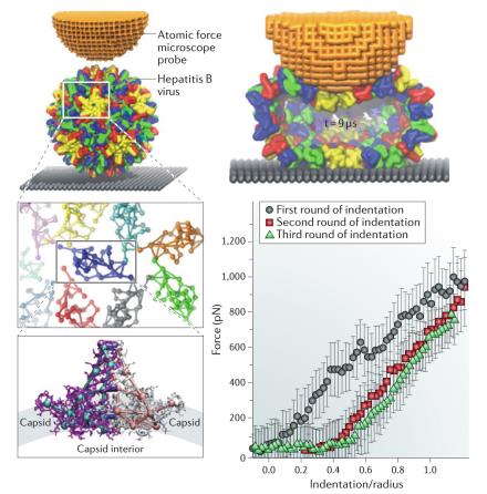 Figure 1. Molecular dynamics simulation of the deformation of a hepatitis B virus by an atomic force microscope probe. (Krieg M, et al., 2019)
What Can We Offer?
With rich testing experience and advanced technical equipment, Creative Biostructure provides customers with various AFM testing services and selects the appropriate testing method according to the needs and purposes of customers.
- Magnetic Force Microscope (MFM)
Magnetic force microscopy (MFM) is an AFM that scans a magnetic sample with a magnetic probe and detects the interaction between the probe and the magnetic sample surface to reconstruct the magnetic structure of the sample surface. The MFM uses a magnetic probe (Si) coated with a layer of magnetic Co-Cr alloy and uses a non-contact mode for detection.
- Lateral Force Microscope (LFM)
The main mode of action of LFM is to make the probe contact with the sample surface and translate on the surface and use the surface friction force of the sample and the deflection of the cantilever caused by the fluctuation of the sample surface to detect the material and surface characteristics of the sample. LFM can be used to measure surface material heterogeneity and generate images with enhanced topographical feature edges.
- Electrostatic Force Microscopy (EFM)
EFM is a scanning probe microscope that uses the electrostatic interaction between the probe and the sample to characterize the electrostatic potential energy, charge distribution, and charge transport on the sample. EFM, like MFM, relies on LiftMode, a two-pass scan technique that performs line scans at the TappingMode on the sample surface and at a specified height above the surface.
- Piezoelectric Force Microscopy (PFM)
Piezoresponsive materials are a class of substances that undergo mechanical deformation when placed under an applied electric field. Piezoresponsive materials have a variety of properties and have a wide range of applications in fields ranging from microelectromechanical systems (MEMS) to biosensors. PFM enables high-resolution nanoscale characterization and topography imaging of piezoelectrically responsive materials.
- Conductive AFM (C-AFM)
C-AFM is a secondary imaging modality derived from "contact mode" that characterizes conductivity changes in medium to low conductivity and semiconducting materials. It can be used to measure and image currents in the 2pA to 1µA range while collecting topographical information.
- PeakForce TUNA AFM
The PeakForce TUNA AFM is ideal for testing the conductivity of fragile samples such as organic photovoltaic cells, conductive nanotubes, and nanoparticles. The PeakForce TUNA provides direct, precise force control and eliminates lateral forces, making high-sensitivity, high-resolution current imaging a routine.
Our Workflow of AFM Applications
Our AFM service begins with a consultation to understand your research goals and sample suitability. We assist in sample preparation and meticulously set up our advanced AFM instruments. We then perform imaging and data acquisition, with an optional force spectroscopy step if needed. Data analysis is conducted, and results are presented in a clear report. We prioritize open communication, offering a consultation to discuss findings and guide further research if required. Our workflow is tailored to ensure high-quality data and support your specific research needs.
Advantages of Our AFM Services
- Expertise: Our team of experienced scientists and researchers are well-versed in AFM applications, offering insightful guidance and support throughout your research.
- High Precision Analysis: Our specialized AFM instruments provide exceptionally precise data, allowing for detailed examination of surface topography and mechanical properties at the nanoscale.
- Quantitative Data: We deliver quantitative data on critical parameters such as surface roughness, adhesion forces, and material properties, facilitating in-depth analysis.
- Custom Solutions: We tailor our services to meet the unique requirements of your research, ensuring that your specific objectives are effectively addressed.
- Rapid Turnaround: We maintain a streamlined workflow to provide prompt results without compromising on the quality of data, allowing you to advance your research with minimal delay.
- Comprehensive Support: Our experts are available to answer your questions, offer guidance, and assist you in making the most of your AFM data.
Creative Biostructure can provide you with various AFM applications. Please don't hesitate to contact us for a detailed quote.
Ordering Process

References
- Li C, et al. Simultaneous electrical and mechanical property mapping at the nanoscale with PeakForce TUNA. Bruker application note AN132 Rev. A, 2011.
- Higuchi S, et al. A quadruple-scanning-probe force microscope for electrical property measurements of microscopic materials. Nanotechnology. 2011, 22(28): 285205.
- Brown B P, et al. Conductive‐AFM Patterning of Organic Semiconductors. Small. 2015, 11(38): 5054-5058.
- Krieg M, et al. Atomic force microscopy-based mechanobiology. Nature Reviews Physics. 2019, 1(1): 41-57.

